价 格
订货量
¥0.40
1 - 99
¥0.30
100 - 9999
¥0.20
价格为商家提供的参考价,请通过"获取最低报价"
获得您最满意的心理价位~
≥10000
| 品牌:嘉泰姆 | 型号:CXSD6209A | 类型:驱动IC |
| 驱动芯片类型:DC转换 | 针脚数:8 | 用途:手机 |
| 封装:SOP8 | 系列:电源 | 功率:10 |
| 批号:2018+ | 特色服务:现货,厂家直销售 | 产品说明:价格优惠,性价比高 |
| 货号:1030 | 是否跨境货源:否 | 包装:盘装 |
| 应用领域:***/航天、 汽车电子、 网络通信、 安防设备、 医疗电子、 测量仪器、 智能家居、 家用电器、 照明电子、 3C数码、 广电教育、 物联网IoT、 可穿戴设备、 新能源 |
目录
1.产品概述 2.产品特点
3.应用范围 4.下载产品资料PDF文档
5.产品封装图 6.电路原理图
7.功能概述 8.相关产品
一,产品概述(General Description)
The CXSD6209A is a current mode monolithic buck switching regulator. Operating with an input
range of 3.6-40V, the CXSD6209A delivers 2A of continuous output current with two integrated N-Channel
MOSFETs.
The CXSD6209A internal synchronous power switches provide high efficiency without
the use of an external Schottky diode. At light loads, regulators operate in low frequency to
maintain high efficiency and low output ripple. Current mode control provides tight load transient response
and cycle-by-cycle current limit.
The CXSD6209A guarantees robustness with short-circuit protection, thermal protection,
start-up current run-away protection, and input under voltage lockout.
The CXSD6209A is available in 8-pin ESOP package, which provides a compact solution with
minimal external components. The package has an exposed pad for low thermal resistance
二.产品特点(Features)
3.6V to 40V operating input range
2A output current
Up to 94% efficiency
High efficiency (>78%) at light load
Internal Soft-Start
Fixed 120kHz Switching frequency
Input under voltage lockout
Available in thermally enhanced ESOP8 package
Start-up current run-away protection
Short circuit protection
Thermal protection
三,应用范围 (Applications)
1.Distributed Power Systems
2.Networking Systems
3.FPGA, DSP, ASIC Power Supplies
4.Green Electronics/ Appliances
5.Notebook Computers
四,下载产品资料PDF文档
需要详细的PDF规格书请扫一扫微信联系我们,还可以获得免费样品以及技术支持!

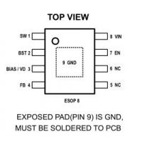
五,产品封装图 (Package)
SOP8 | Name | Description |
1 | SW | SW is the switching node that supplies power to the output. Connect the output LC filter from SW |
2 | BST | Bootstrap pin for top switch. A 0.01uF or larger capacitor should be connected between this pin |
3 | VD | Output of the internal LDO. A capacitor of 2.2uF or larger should be connected at VD to ground. |
4 | FB | Output feedback pin. FB senses the output voltage and is regulated by the control loop to 0.8V. |
5 | NC | |
6 | NC | |
7 | EN | Drive EN pin high to turn on the regulator and low to turn off the regulator. |
8 | VIN | Input voltage pin. VIN supplies power to the IC. Connect a 3.6V to 40V supply to VIN and bypass |
9 | GND | Ground. |
六.电路原理图
七,功能概述
八,相关产品 更多同类产品......